I2C - Master read v1
I2C - Master read v1 — The I2C Master read driver
block allows data to be read from a slave device supporting the I2C slave
protocol. One block is required for each channel to be read. Multi-master mode
and clock stretching are currently not supported.
Library
Simulink Real-Time - Speedgoat
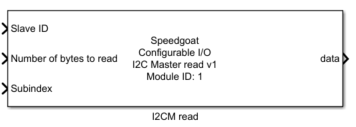
Description
The I2C Master read driver block allows data to be read from a slave device
supporting the I2C slave protocol.
One block is required for each channel to be read. Multi-master mode and clock
stretching are currently not supported.
Ports
This driver block has three inputs, and one output port.
Inputs
-
Slave ID
7-bit identifier to access the I2C Slave node.
-
Number of Bytes to Read
Defines the number of bytes to read. Possible values (limited by the
hardware buffer size) are between 0 and 256.
-
Subindex
The I2C master can send a first byte to configure the slave. This
input is available when the Enable Subindex
Configuration parameter is checked.
Outputs
-
Data
The data retrieved.
-
Ack Error
Displays the error flag related to I2C acknowledge. This port is only
available when the Show Acknowledge Error
Port parameter is enabled.
Parameters
Tab: Module setup
-
Configurable I/O Module ID
This parameter associates a code module block with a configurable I/O module setup
block. Set this value to match the Module ID defined in the setup block of the
required configurable I/O module.
-
Channel
The number of the channel which this driver block entity will access. Only one
channel per driver block can be addressed. You can specify channels in the range 1-N
(N = the number of channels implemented in your specific configuration file defined
in the Setup block).
-
Sample Time
Defines the base sample time at which this driver block gets its sample hit. This
parameter can also be set to -1 for inherited
sample time. The units are in seconds.
Tab: I2CM
-
I2C Clock Rate
Configures the I2C transmission clock rate. When selecting Custom, any rate between
fFPGA/8 and fFPGA/
(216 − 1) can be specified. The rate is
derived from the FPGA frequency using a clock divider; therefore, exact
rates across the full specified range cannot always be achieved. The
effective rate and the corresponding relative error are
displayed.
Example: If the FPGA frequency is 75 MHz, then the corresponding
frequency range is approximately 9.375 MHz to 1.144 kHz.
-
Read Value From Previous Model Step
By checking this parameter, the driver output Data will indicate the I2C data received from the
previous model step. This option reduces the TET. Otherwise, the driver
actively waits for the I2C transfer (which increases the TET) to be
finished and then the output Data
contains the I2C data received from the current model step (for details
see I2C Read Value from Previous Model Step)
Tab: Input and Output Port Configuration
-
Enable Subindex Configuration
By checking this parameter, an additional input becomes available
which allows you to write one byte to the slave device before the read
operation is initiated. This is useful if a register address to read
from should be set before the read-operation will be done. (for details
see I2C
Read with Subindex)
-
Show Acknowledge Error Port
By checking this parameter, an additional output becomes available
which indicates the status of the acknowledge flag (1: error, 0: no
error).