SSI - Master v2
SSI - Master v2 — The SSI Master driver block
enables data to be read from an SSI encoder.
Library
Simulink Real-Time - Speedgoat
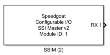
Description
The SSI Master (Decoder) driver block enables data to be read from a SSI Slave
(Encoder).
At each time step of the Simulink model, the driver block reads the most recent
value that has been received.
Ports
This driver has a number of output ports corresponding to the number of active
channels.
The output ports provide the value read by the SSI Master module.
Parameters
Tab: Module setup
-
Configurable I/O Module ID
This parameter associates a code module block with a configurable I/O module setup
block. Set this value to match the Module ID defined in the setup block of the
required configurable I/O module.
-
Channel Vector
A vector of channels this driver block entity will access. You can specify
channels in the range 1-N (N = the number of channels implemented in your specific
configuration file defined in the Setup block). The width of this vector also
defines the subsequent size of some of the following parameters if scalar expansion
applies. With a single block, all the channels of the block are synchronized.
-
Sample Time
Defines the base sample time at which this driver block gets its sample hit. This
parameter can also be set to -1 for inherited
sample time. The units are in seconds.
Tab: SSIM configuration
-
Decoding
Whether the input signal is coded in Binary or Gray code.
-
Data Size
The number of bits used in the transmission (32 or 64 bits maximum
depending on the module version). This value must consider the number of
all the bits read by the master, including possible start/stop and
parity bits (see Timing Diagram).
-
Frequency
Configures the SSI clock rate in Hz. The maximum frequency is the FPGA
frequency divided by 10.
Example: FPGA frequency is 75 MHz → the corresponding maximum
frequency is 7.5 MHz.
-
Time pause
The length of the TP delay (see Timing Diagram) in seconds. This must be greater than a
single SSI data period (greater than 1/Frequency).
-
Time low
The length of the TL delay (see Timing Diagram) in seconds. This parameter is only
available if SSI2 Decoding is selected.
This time must be greater than a single SSI data period (greater than
1/Frequency).
-
SSI2 Decoding
Check this box if the SSI Master module will be used to read an SSI2
encoder. In this case the MSB and LSB of the read frame are reversed
compared to a standard SSI encoder.
-
Mode
Free run:If selected, the SSI Master
continuously generates the SSI clock signal that defines the SSI frame.
As soon as the Time pause (TP) is
finished, the next frame starts immediately. The SSI frame is not
synchronized to the model sample rate of the driver block in this
mode.
Every time the driver block is executed in a simulation step, the SSI
data received from the previously completed SSI frame will be available
on the RX-values output port. See Timing Diagram of Free run
mode
Synchronization (no waiting time): If
selected, the SSI Master starts the transmission of a single SSI frame
every time the driver block is executed during a simulation step and if
the SSI frame is idle. If the SSI frame is not idle, no new SSI frame is
triggered, and the ongoing SSI frame is not aborted.
Every time the driver block is executed in a simulation step, the SSI
data received from the previously completed SSI frame will be available
on the RX-values output port. Refer to the following timing diagrams:
Synchronization No Waiting Time (tFrameSSI
<
tSample) and Synchronization No Waiting Time
(tFrameSSI
> tSample)
Synchronization (waiting time
applicable): If selected, the SSI Master starts the
transmission of a single SSI frame every time the driver block is
executed during a simulation step. The driver block then actively waits
until the SSI frame is finished. The SSI data from this frame are then
available on the RX-values output port within the same simulation
step.
![[Note]](images/note.png) | Note |
|---|
This mode represents fully synchronized behavior. The task
execution time is higher due to the driver actively waiting for the
complete SSI frame to be finished. The simulation step time must
therefore be greater than the duration of a complete SSI frame
(including Time pause), otherwise a
CPU-overload will occur. |
| Note |
|---|
The FPGA clock frequency and the corresponding time of a tick can be found in the
Setup block. |
| Note |
|---|
Values expressed in seconds and hertz will be rounded to the FPGA resolution.
For instance, if FPGA base clock is equal to 75[MHz], then the resolution is
13.33[ns]. |
| Note |
|---|
From version v2.7 and later, the output data type will be uint64 if the
Data Size parameter is > 32bit. This is
considered a fixed-point data type by Simulink and cannot be interpreted by the
scope block. Either use the data conversion block or view the output data in the
data inspector. |