SPI - Master / Slave v1
SPI - Master / Slave v1 — The SPI driver block can act
as SPI Master or SPI slave.
Library
Simulink Real-Time - Speedgoat
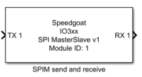
Description
The SPI driver block can act as SPI Master or SPI slave.
Ports
Inputs
-
TX n (n is the channel number)
Definition of the frame to send. The number of elements of the input
vector is defined with the frame size parameter in the SPI Configuration tab. Each element of the
input data vector corresponds to a SPI data word.
Outputs
-
RX n (n is the channel number)
Gives access to data from the MiSo or MoSI I/O line, depending on
which role (Master or Slave) was selected. This port is enabled by
ticking the Show RX outputs checkbox.
As this will introduce additional latency, it is good practice to only
check this box if such data is required.
Parameters
Tab: Module setup
-
Configurable I/O Module ID
This parameter associates a code module block with a configurable I/O module setup
block. Set this value to match the Module ID defined in the setup block of the
required configurable I/O module.
-
Channel
The number of the channel which this driver block entity will access. Only one
channel per driver block can be addressed. You can specify channels in the range 1-N
(N = the number of channels implemented in your specific configuration file defined
in the Setup block).
-
Sample Time
Defines the base sample time at which this driver block gets its sample hit. This
parameter can also be set to -1 for inherited
sample time. The units are in seconds.
Tab: SPI Configuration, Master Role
-
CPOL
The clock polarity parameter:
-
CPHA
The clock phase parameter
-
Role
Role of the SPI module.
Tab: SPI Configuration, Master Role
-
Clock Divider
Clock rate of the SCLK I/O line, in reality the duration of the SCK
half period (Parameter T2 of the timing diagram in the
Usage Notes). The FPGA counts from 0 to the clock divider
value, e.g. for a value of 5, the clock output will be low for ticks 0,
1, 2, 3, 4 and 5 (this makes a total of 6 effective FPGA ticks) and then
the clock output will be high for the following ticks 0, 1, 2, 3, 4 and
5. Valid range is 1 to 232-1.
-
Start Delay
Time between the end of a start condition, and when the frame is sent.
The units are in ticks. Valid range is 0 to 65535.
-
Interwords Delay
Idle time between words of a single frame. The units are in ticks.
Valid range is 0 to 65535.
-
Stop Delay
Time between sending the last bit and entering the stop condition
state. The units are in ticks. Valid range is 0 to 65535.
-
Number of Bits per Word
Defines the size of the words. Valid range is 1 to 32 (see Note under
"Number of Words per Frame").
-
Number of Words per Frame
Defines the count of words which are sent in a frame. Valid range is 1
to 32 (see Note immediately below).
![[Note]](images/note.png) | Note |
|---|
The maximum number of bits per SPI transition is limited to 256
bits. Therefore, the product of Number of Bits
per Word x Number of Words per
Frame may not be greater than 256. |
-
Line Delay Compensation
Defines the phase shift between the emitted clock and internal clock
used to sample slave information. The units are in ticks. Valid range is
0 to 15.
Tab: SPI Configuration, Slave role
-
Word Size Vector
Defines the size of the words. Valid range is 1 to 32 (see Note under
"Number of Words per Frame").
-
Frame Size Vector
Defines the count of words which are sent in a frame. Valid range is 1
to 32 (see Note under "Number of Words per Frame").
Tab: Input and Output Configuration
-
Show RX Outputs
When this checkbox is enabled, data read on the MiSo I/O line will be
available in Simulink via a dedicated output port. Enabling this
checkbox introduces additional latency due to additional data transfer.
Only enable this parameter if absolutely necessary.
-
Show TX Outputs
When this checkbox is enabled, data sent on the MoSi I/O line will be
available in Simulink via a dedicated input port. Enabling this checkbox
introduces additional latency due to additional data transfer. Only
enable this parameter if absolutely necessary.
| Note |
|---|
The FPGA clock frequency and the corresponding time of a tick can be found in the
Setup block. |