IO421 - LVDT/RVDT Write
IO421 - LVDT/RVDT Write —
Writes the IO421 LVDT/RVDT outputs
Library
Simulink Real-Time - Speedgoat
Description
The IO421-3 sub-module simulates up to three Linear or Rotary Variable
Differential Transformers. Each simulated device consists of a primary coil, which
requires a reference alternating current, and two secondary coils. The output
voltages of the secondary coils depend on the position of the ferromagnetic rod. You
can define the position in the Simulink model, using the LVDT write driver
block.
The characteristics of the sub-module depend on the factory configuration selected
at the time of the order. This information is available in a separate documentation
shipped with the device.
See section IO421-3 LVDT/RVDT connection methods in the 'Usage notes' section for
more information about the various connection methods.
Ports
Inputs
-
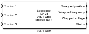
Position n (n is the channel number)
The position of the ferromagnetic rod during the simulated runtime.
The input value is limited to the supported range which is between
-0.995 and +0.995. The number of these ports is dependent on the channel
count, which is specified by the 'Channels vector' parameter.
-
Excitation
Set the expected reference (R inputs) voltage in (V RMS). The voltage
range depends on the submodule code of your I/O module.
-
VLL Voltage
Set the line to line output voltage of the A/B signals in (V RMS). The
voltage range depends on the submodule code of your I/O module.
-
Phase Offset
Set the phase offset between A/B output and the reference signal in
degrees [ ° ]. The parameter can be defined with an accuracy of 0.1° and
the range is -90° to 90°.
Outputs
-
Wrapped position
Position data based on A/B value. This port is enabled or disabled in
the 'Input and output ports configuration' tab of this block's dialog
box. The width of this port is dependent of the number of channels
(defined by the 'Channels vector' parameter).
-
Wrapped frequency
The frequency of the reference (excitation) signal. This port is
enabled or disabled in the 'Input and output ports configuration' tab of
this block's dialog box. The width of this port is dependent of the
number of channels (defined by the 'Channels vector' parameter).
-
Wrapped voltage
The voltage of the reference (excitation) signal. This port is enabled
or disabled in the 'Input and output ports configuration' tab of this
block's dialog box. The width of this port is dependent of the number of
channels (defined by the 'Channels vector' parameter).
-
Status
Status information for this module. This parameter is a vector of 4
binary elements. Each element represents a fault. A value of 0 indicates
that no fault is present, and 1 indicates a fault. The faults are as
follows (in order of position within the vector):
The signal is below 90% of the expected threshold, and
signal loss occurs.
The reference is below 90% of the expected
threshold.
The built-in tests have failed.
Reference phase has been lost.
This port is enabled or disabled in the 'Input and
output ports configuration' tab of this block's dialog box.
All ports are vectors. The width of the vector, and the order of the corresponding
channels, is dependent on the configuration of the 'Channel vector'
parameter.
Parameters
Tab: Module Setup
-
Module ID
A unique module ID must be used for each type of IO421 module block in
your model.
The module ID has two functions:
It defines the logical connection to link the I/O module
driver blocks with each other
It also has an impact on the PCI slot auto-search feature: if
only one I/O module is installed, the module ID must be set to
1. If multiple modules are
installed, it must be in the range 1:n. Not all the I/O modules
installed in the target machine need to be used
-
Slot
The carrier board can contain up to three sub-modules. This parameter
indicates where is your IO421-1 located.
-
Active Channels
Select the active input/output channels in a vector. A defined number of channels
can be selected using square brackets, for example [1 2 3]. A sequence of channels
can be selected using a colon, for example, 1:4.
-
Sample Time
Defines the base sample time at which this driver block gets its sample hit. This
parameter can also be set to -1 for inherited
sample time. The units are in seconds.
-
PCI Slot (-1: auto-search)
There are two approaches for mapping this block to a specific I/O module installed
in your target machine. All modules of the same type must be configured using the
same method.
Auto-Search: with the default value -1 the I/O module will be automatically located in the
target machine. If you have multiple modules of the same kind, the
Module ID defines which module is associated with this block. To see how
each I/O module maps to a Module ID, use this Speedgoat API:
speedgoat.getIoInterfaces("TargetName", "mySpeedgoat")
Explicit Addressing: to explicitly define the logical address of the
I/O module in the target machine, you can provide the PCI bus and slot
numbers as a vector: [bus, slot]. To determine these numbers, run the
following command in the MATLAB command window:
speedgoat.getIoInterfaces("TargetName", "mySpeedgoat", "Advanced", true)Note
that the PCI address can change whenever an I/O module is added or
removed – usually, auto-search is the best option.
Tab: Input and Output ports Configuration
-
Show Status Output Port
When checked the 'Status' output port is enabled.
-
Show "Wrapped frequency" Output Port
When checked the 'Wrapped reference frequency' output port is enabled.
-
Show "Wrapped voltage" Output Port
When checked the 'Wrapped reference voltage' output port is enabled.
-
Show "Wrapped position" Output Port
When checked the 'Wrapped position' output port is enabled.
-
Show Excitation Voltage Input Port
When checked the excitation input port is enabled.
-
Show VLL Voltage Input Port
When checked the VLL voltage input port is enabled.
-
Show Phase Offset Input Port
When checked the phase offset input port is enabled.
Tab: Excitation
-
Expected Excitation Voltage VREF Vector
This parameter informs the IO421 I/O module about the expected
reference (R inputs) voltage in (V RMS). You can either use a scalar
value, which applies to all channels, or a vector which is mapped to the
Channels vector.
![[Note]](images/note.png) | Note |
|---|
The phase lock between the excitation and the signal output can
take up to 1 second after connecting a valid excitation signal or
starting the model. Consequently, no signals are immediately present
at the output. |
Tab: A/B Output
-
Wiring Mode Vector
Define if the LVDT simulator is connected in 2-wire or 4-wire mode.
For 3-wire connections, select 4-wire mode. See IO421-1 LVDT/RVDT
connection methods for more information about the wiring. Define either
a vector which will be mapped to the Channels vector, or a scalar which
applies to all channels.
-
VLL Output Mode Vector
Select either '0' for ratio-metric output or '1' for fixed output. In
ratio-metric mode, the output reflects changes in the excitation
voltage, based on the ratio defined by VLL output voltage / Expected
excitation voltage. V OUT = V REF IN * (VLL output voltage / Expected
excitation voltage) In fixed mode, the changes in the excitation voltage
are not reflected on the outputs. The value of VLL output voltage
defines the voltage of the outputs. Define either a vector which will be
mapped to the Channels vector, or a scalar which applies to all
channels.
-
VLL Output Vector
This parameter configures the line to line output voltage of the A/B
signals in (V RMS). Define either a vector which will be mapped to the
Channels vector, or a scalar which applies to all channels.
-
Phase Offset Vector
This parameter defines the phase offset between A/B output and the
reference signal in degrees [ ° ]. The parameter can be defined with an
accuracy of 0.1°.