BiSS - Encoder v1
BiSS - Encoder v1 — The BiSS Encoder code module
acts as the slave implementation of the BiSS communication. The driver block can
be configured for generic support of different BiSS encoders and
setups.
Library
Simulink Real-Time - Speedgoat
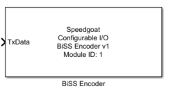
Description
The BiSS Encoder code module acts as the slave implementation of the BiSS
communication. The driver block can be configured for generic support of different
BiSS encoders and setups.
The following sections describe the code module in more detail:
Usage notes
Input and output ports
Dialog fields
Ports
This BiSS Encoder driver block has no outputs, and up to four input ports.
Outputs
-
TxData
The data value to be sent to the BiSS master.
-
CRC
The value of the BiSS CRC bits specified in the configuration.
-
Warning
The value of the BiSS Warning flag.
-
Error
The value of the BiSS Error flag.
Parameters
Tab: Module setup
-
Configurable I/O Module ID
This parameter associates a code module block with a configurable I/O module setup
block. Set this value to match the Module ID defined in the setup block of the
required configurable I/O module.
-
Channel Vector
A vector of channels this driver block entity will access. You can specify
channels in the range 1-N (N = the number of channels implemented in your specific
configuration file defined in the Setup block). The width of this vector also
defines the subsequent size of some of the following parameters if scalar expansion
applies. With a single block, all the channels of the block are synchronized.
-
Sample Time
Defines the base sample time at which this driver block gets its sample hit. This
parameter can also be set to -1 for inherited
sample time. The units are in seconds.
Tab: BiSS configuration
-
Line Delay Vector
Configures the Line Delay time introduced on the data line. This
allows to emulate the line delay introduced by a long cable. E.g. if we
define a value of [10], the data will be delayed for 10 FPGA ticks.
Units are in ticks. Valid range 0 to 1000, which corresponds to a line
delay of approx. 0 to 13.34us.
-
Busy Delay Vector
Configures the Busy Delay time introduced on the data line. The busy
delay allows the slave to take more time for e.g. calculations before
the data is sent. E.g. if we define a value of [10], the start bit will
be delayed for 10 FPGA ticks. Units are in ticks. Valid range 0 to 3000.
-
Timeout Time Vector
Configures the BiSS Encoder timeout time. The BiSS Encoder starts
measuring the timeout at the last rising edge on the clock. Once
expired, a rising edge at SLO flags the timeout to the BiSS Decoder.
Common times are set to 40 us, which corresponds to 3000 ticks @ 75
MHz FPGA frequency.
-
Data Bits Vector
The number of BiSS data bits. Additional transmission bits like
Warning, Error and CRC are configured separately. The valid range is 0
to a maximum of 64 (the maximum depends on the additional flag and CRC
port settings).
-
Error Flag
Configures an Error flag port.
-
Warning Flag
Configures a Warning flag port.
-
CRC Bits
Configures the CRC bits port.
-
Number of CRC Bits
Configures the number of CRC Bits. Valid range 0 to 8.
![[Note]](images/note.png) | Note |
|---|
The Error Flag, Warning Flag and the CRC Bits are concatenated with the data
bits into the BiSS frame. The code module does not calculate a CRC
value. |
| Note |
|---|
The FPGA clock frequency and the corresponding time of a tick can be found in the
Setup block. |