BiSS - Decoder v1
BiSS - Decoder v1 — The BiSS code module acts as the
master implementation of the BiSS communication. The driver block can be
configured for the generic support of different BiSS
Encoders.
Library
Simulink Real-Time - Speedgoat
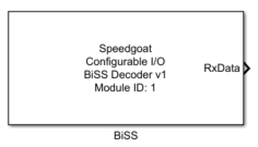
Description
The BiSS code module acts as the master implementation of the BiSS communication.
The driver block can be configured for the generic support of different BiSS
Encoders.
The following sections describe the code module in more detail:
Usage notes
Ports
Dialog fields
Ports
This BiSS driver block has no inputs, and up to five output ports.
Outputs
-
RxData
The data value received from the encoder.
-
CRC
The value of the BiSS CRC Bits
specified in the configuration.
-
Warning
The value of the BiSS Warning Flag.
-
Error
The value of the BiSS Error Flag.
-
TrsmErr
Indicates whether the BiSS data transmission was successful (0) or
corrupted (1).
Parameters
Tab: Module Setup
-
Configurable I/O Module ID
This parameter associates a code module block with a configurable I/O module setup
block. Set this value to match the Module ID defined in the setup block of the
required configurable I/O module.
-
Channel Vector
A vector of channels this driver block entity will access. You can specify
channels in the range 1-N (N = the number of channels implemented in your specific
configuration file defined in the Setup block). The width of this vector also
defines the subsequent size of some of the following parameters if scalar expansion
applies. With a single block, all the channels of the block are synchronized.
-
Sample Time
Defines the base sample time at which this driver block gets its sample hit. This
parameter can also be set to -1 for inherited
sample time. The units are in seconds.
Tab: BiSS Configuration
-
Clock Divider Vector
Configures the BiSS transmission clock rate in FPGA clock ticks; for
example, if we define a value of [10], the clock line will be low for 10
ticks, and high for 10 ticks. The valid range is 6 to 468.
Example: FPGA frequency is 75MHz the corresponding frequency range is
approximately 6.25MHz to 80kHz.
-
Timeout Time Vector
Configures the maximum permitted BiSS timeout time. After the last
rising edge on the clock line, the BiSS Decoder waits for the configured
timeout time before a new transmission can start. During the timeout
time, the connected BiSS Encoder must go to idle state (rising edge on
SLO).
The same timeout time is used to detect a timeout on SLO, for example
when the BiSS Encoder does not respond. If a timeout occurs, the
Show Transmission Error output will
go high.
Common times are set to 40 us, which corresponds to 3000 ticks @
75 MHz FPGA frequency.
-
Data Bits Vector
The number of BiSS data bits. Additional transmission bits such as
Warning, Error and CRC are
configured separately. The valid range is 0 to a maximum of 64 (the
maximum depends on the additional flag and crc port settings).
-
Error Flag
Configures an Error Flag port.
-
Warning Flag
Configures a Warning Flag port.
-
CRC Bits
Configures the CRC Bits port.
-
Number of CRC Bits
Configures the number of CRC Bits.
The valid range is 0 to 8.
![[Note]](images/note.png) | Note |
|---|
The Error Flag, Warning Flag and the CRC Bits are extracted from the received
BiSS frame data. |
-
Show Transmission Error
If checked, the Transmission Error
port is enabled. This port will indicate (1) if an error occurred during
the BiSS data transmission (either timeout or corrupt frame).
-
Full Synchronization
If checked, the BiSS communication is fully synchronized. This means
that in the same sample step the BiSS Decoder starts the communication
and actively waits until all data is received. When unchecked, the BiSS
Decoder does not wait until the end of the communication. It reads the
last valid value (the first value after startup will be invalid). This
can help reduce the task execution time.
| Note |
|---|
The FPGA clock frequency and the corresponding time of a tick can be found in the
Setup block. |