Resolver Emulation v1
Resolver Emulation v1 — The Resolver Emulation
driver block provides the simulation functionality for a
Resolver.
Library
Simulink Real-Time - Speedgoat
Description
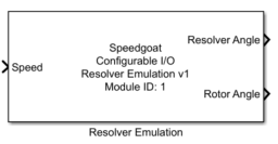
The Resolver Emulation driver block provides the simulation functionality for a
Resolver.
This driver block can only be used in combination with an analog setup block.
Analog settings such as voltage range and trigger selection must be set in the
analog setup block.
Ports
Inputs
-
Speed / Position
This port is used to input the speed at which the Resolver rotates
[rad/s]. By selecting Position in the
mask dropdown, the input will switch its functionality to position input
[rad]. The width of this input signal must be equal to the number of
active channels defined in the Channel
Vector parameter.
-
Gain
The gain represents the transfer ratio between the input and output
windings of the resolver. The resolver emulation code module uses four
single-ended analog outputs to generate quasi-differential signals: sin
(+), sin (-), cos(+), and cos (-). The gain can be set independently for
each output. This input expects a vector, which must contain 4 elements
per active channel.
-
Offset
An independent DC offset voltage can be applied to each of the four
resolver output signals: sin (+), sin (-), cos(+), and cos (-). This
input expects a vector, which must contain 4 elements per active
channel. Each element represents the offset for one of the four resolver
output signals. The unit is [V].
-
Excitation Fault
The excitation input signal of the resolver emulation model is set to
zero if this input goes to 1. The width of this input signal must be
equal to the number of active channels defined in the Channel Vector parameter.
Outputs
The width of each output signal is equal to the number of active channels
defined in the Channel Vector parameter.
-
Resolver Angle
This port shows the angular position of the resolver [rad].
-
Rotor Angle
This port shows the angular position of the rotor [rad].
-
Overshoot Flag
The flags indicate an overshoot of the excitation signal and resolver
output signals.
Parameters
Tab: Module Setup
-
Configurable I/O Module ID
This parameter associates a code module block with a configurable I/O module setup
block. Set this value to match the Module ID defined in the setup block of the
required configurable I/O module.
-
Channel Vector
A vector of channels this driver block entity will access. You can specify
channels in the range 1-N (N = the number of channels implemented in your specific
configuration file defined in the Setup block). The width of this vector also
defines the subsequent size of some of the following parameters if scalar expansion
applies. With a single block, all the channels of the block are synchronized.
-
Sample Time
Defines the base sample time at which this driver block gets its sample hit. This
parameter can also be set to -1 for inherited
sample time. The units are in seconds.
-
Resolver Sample Time
The sample time at which the resolver module is triggered on the FPGA.
The unit is [s].
Tab: Resolver
-
Pole Pairs
The number of resolver pole pairs.
-
Resolver Angle Offset
Angular offset [degree] between the rotor zero position and the zero
position at which the resolver is mounted.
-
Speed / Position Input
The functionality of the Speed / Position input is selected from this
dropdown.
Selecting Speed will rename
the mask input to Speed. The input values will be considered as
speed values in rad/s
Selecting Position will
rename the mask input to Position. The input values will be
considered as position values in rad
-
Initial Position
The initial angular position of the Resolver in degrees. This
parameter is only available if the Speed input has been selected in the
dropdown. If Position is chosen, the initial position will be read from
the mask input.
-
Use Internal Excitation Signal
If checked, the Resolver will use the internally generated excitation
signal. The signal characteristics are defined with the Excitation Amplitude and Excitation Frequency parameters. These
parameters are visible when the checkbox is selected.
-
Excitation Amplitude
Amplitude of internal excitation signal [V].
-
Excitation Frequency
Frequency of internal excitation signal [kHz].
-
Initial Gain
The gain represents the transfer ratio between the input and output
windings of the resolver. The resolver emulation code module uses four
single-ended analog outputs to generate quasi-differential signals: sin
(+), sin (-), cos(+), and cos (-). The gain can be set independently for
each output. This parameter expects a scalar value or a vector of 4
elements per active channel; for example, set the parameter to '[0.5,
0.5, 0.5, 0.5, 1, 1, 1, 1]' if you have two active resolver emulation
channels. The first resolver will have a transfer ratio of 0.5 and the
second one a transfer ratio of 1.
The Initial Gain applies a). when the
model is initialized; and b). until the first model step, if the
Gain input is active. If the
Gain input is disabled, the
Initial Gain applies during the
entire model execution.
-
Initial Offset
An independent DC offset voltage can be applied to each of the four
resolver output signals: sin (+), sin (-), cos(+), and cos (-). This
parameter expects a scalar value or a vector of 4 elements per active
channel containing the offset for each of the four resolver output
signals. The unit is [V]. For example, set the parameter to
'[2,2,2,2,1,1,1,1]' if you use two resolver emulation channels and you
want an offset of 2 V for all the outputs of channel 1 and an offset of
1 V for all the outputs of channel 2.
The Initial Offset applies a). when
the model is initialized; and b). until the first model step, if the
Offset input is active. If the
Offset input is disabled, the
Initial Offset applies during the
entire model execution.
-
Phase Delay [Degree]
Phase delay between the excitation input signal and the modulated sine
and cosine outputs.
-
Phase Delay[FPGA Model Sample Steps]
Number of resolver model sample steps for which the excitation signal
is delayed. This parameter is automatically computed and shown by the
driver block based on the defined phase delay in degrees.
Tab: Input and Output Port Configuration
-
Show Offset Input
When this parameter is set, the
Offset input is shown.
-
Show Gain Input
When this parameter is set, the Gain
input is shown.
-
Show Excitation Fault Input
When this parameter is set, the Excitation
Fault input is shown.
-
Show Overshoot Flag Output
When this parameter is set, the Overshoot Flag
output is shown.
-
Show Rotation Angle Output
When this parameter is set, the Rotation Angle
output is shown.
-
Show Resolver Angle Output
When this parameter is set, the Resolver
Angle output is shown.